Hardware / PCB Design
PCB Design
Schematic capture and board layout, from a first concept to a board that is actually manufacturable — and then assembled, powered up, measured and revised here, rather than handed off as a Gerber with fingers crossed.
What this covers
- Schematic capture and part selection
- Mixed-signal and high-speed layout
- Power tree and signal integrity
- Fine-pitch placement and reflow in-house
- Design for manufacture and test
- Bring-up, measurement and revision
Why that last part matters
A layout is a hypothesis. It stops being one the first time you power the board.
Plenty of people can produce a compliant layout. The design rules pass, the netlist matches, the Gerbers export. What that does not tell you is whether the return path under the fast signal is intact, whether the regulator will be stable with the capacitor that was actually available, or whether the connector fouls the enclosure by half a millimetre.
Those things are discovered by building the board and measuring it. When layout, assembly, bring-up and fault-finding stay in the same hands, the correction lands in the next revision instead of in an email thread between three companies about whose fault it was.
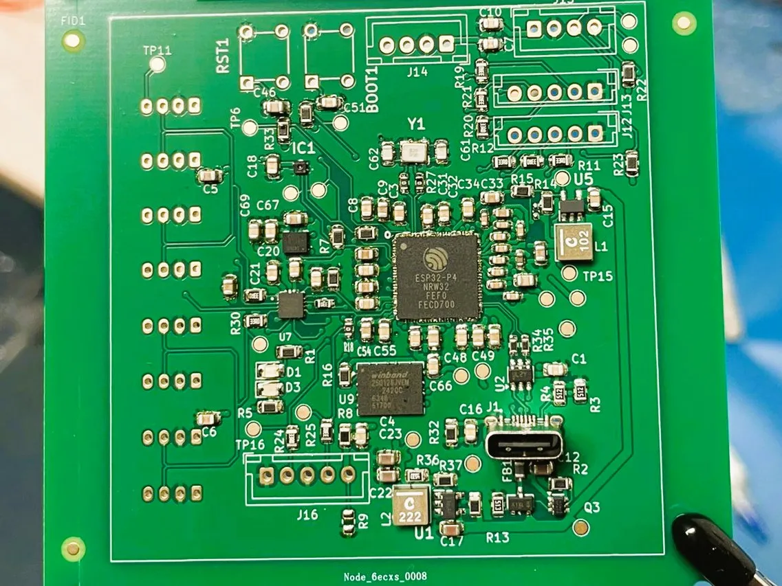
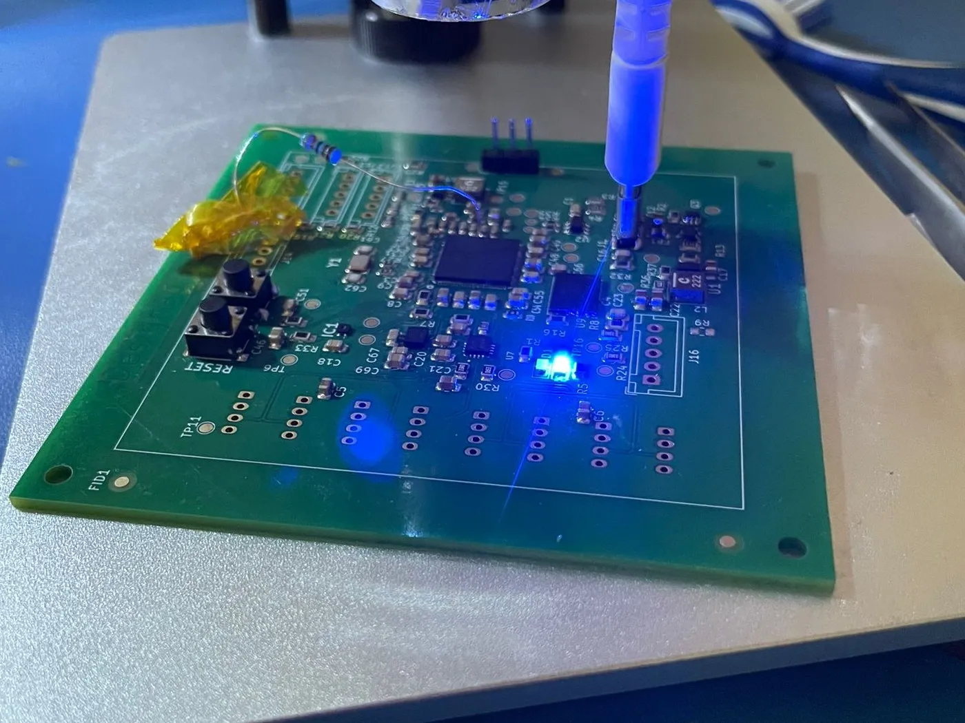
Boards we have designed and built
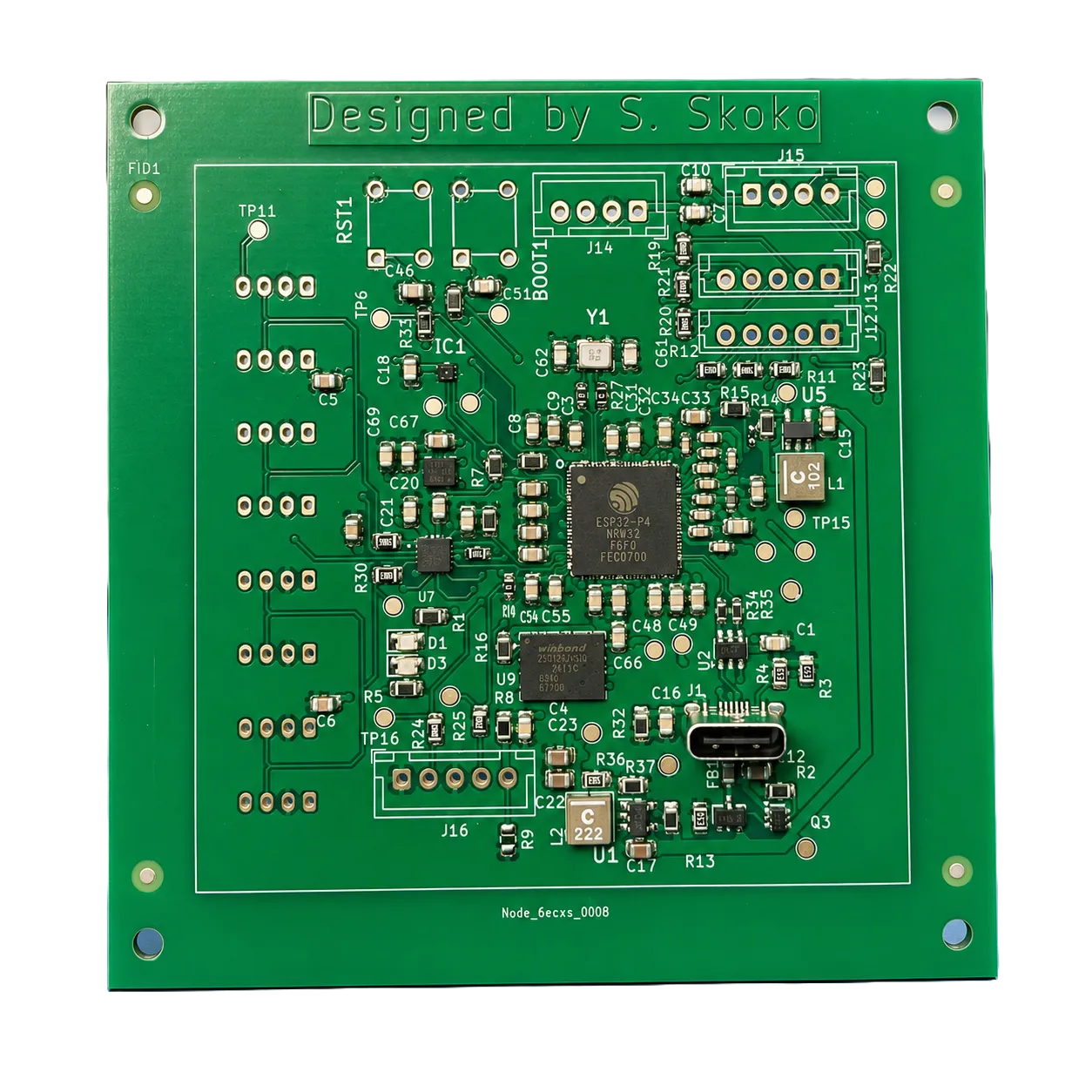
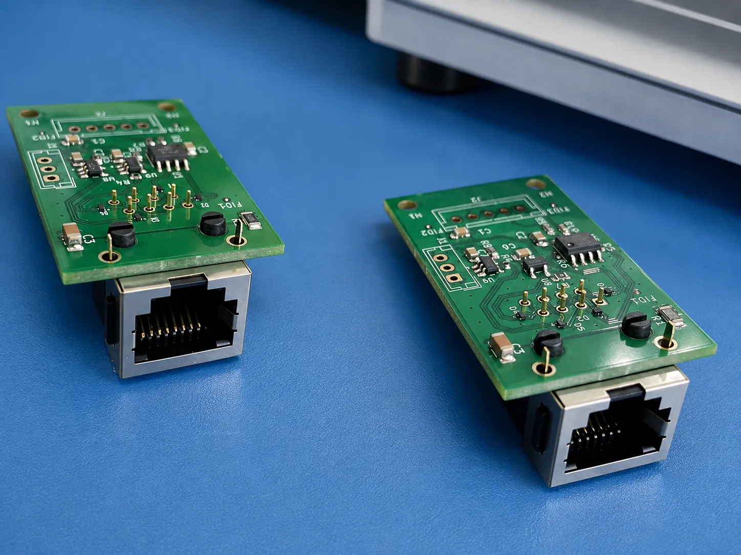
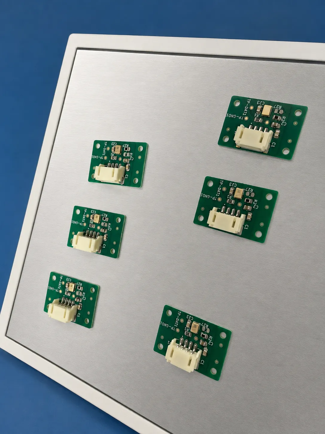
Three designs for our own sensing platform, each solving a different layout problem: dense fine-pitch placement around a capable controller, a differential link that has to stay clean over fifteen metres of ordinary cabling, and a small board repeated eight times whose mechanical position is part of the acoustic design. All were sourced, assembled and brought up here, and all have been through at least one revision driven by what the bench showed.
See what was measured with them →What the work covers
Schematic capture
Circuit design with the part selection made alongside it, because a schematic drawn around components you cannot buy is a drawing, not a design.
Part selection and BOM
Chosen for availability, lifecycle and second sources as much as for datasheet performance — with the sourcing reality checked before the layout depends on it.
Layout
Placement and routing against the physics: return paths, controlled impedance where it matters, power integrity, thermal behaviour, and keeping sensitive analog away from the noisy parts.
Mixed-signal and fine pitch
Analog front ends next to digital switching, and packages down to 0.35 mm pitch placed and reflowed in-house.
Design for manufacture and test
Fiducials, test points, clearances and panelisation considered during layout, plus the access you will want when something needs probing later.
Mechanical fit
Board outline, connector positions and mounting developed together with the enclosure, so the two are not discovered to disagree after both are made.
How a board runs here
- 01
Requirements and architecture
What the board must do, under what constraints — power, size, environment, interfaces, cost.
- 02
Schematic and parts
Circuit and bill of materials developed together, availability checked as decisions are made rather than after.
- 03
Layout and review
Placement, routing, and a review pass against the physics as well as the design rules.
- 04
Fabrication and assembly
Boards ordered and populated in prototype quantities here, which keeps the loop between a decision and a physical result short.
- 05
Bring-up and measurement
Power up, prove each subsystem, then measure. Findings are written down, including the inconvenient ones.
- 06
Revision
A second spin informed by the bench. Boards that have never been revised have usually never been tested properly.
What we are not
Not a contract manufacturer: boards are assembled here in prototype quantities for development and testing, not at production volume. When a design is ready for series production we prepare the documentation for it and work with your manufacturer, rather than pretending to be one. We are also not a certification lab — we design with CE, FCC and EMC in mind and prepare for testing, which accredited third parties then carry out.
Related
Have a board that needs designing?
Bring the requirements, or an existing design that is not behaving. You get an honest read on approach, the risks visible from the outside, and whether we are the right people for it.
Discuss a project →